Speedball upgrade - small board: One LED not lighting, one V reading out of spec

Luxifer

New member
I started this upgrade with an in-spec, stock Crack, which I built 1.5 weeks ago.

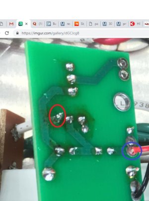
I just installed the smaller board of the speedball upgrade, and had two issues come up while performing voltage checks:

The voltage reading on 0B is out of spec at about 50-51 V, but all of the rest of the voltages are in spec. If it's of significance, all of the rest of the voltages are toward the lower end of the "in-spec" ranges listed in the manual.

Also, the LED closest to 1B is not lighting up. I have tried reflowing the solder on its legs, which didn't help (although maybe I need to try again?).

The three other LEDs are lighting up properly.

I'm guessing that these issues are related, but let me know what I should try, or what you think, please!

Thanks very much!

 
That was exactly it! Voltage is now reading around 71, and all four LEDs on the small board are glowing. I can't believe that you were able to predict that based on two symptoms!

Oddly though, the LED on the 12AU7 socket connecting A3 to the center is no longer lighting up. I accidentally brushed it with my finger while probing it to see if I could figure anything out, and it lit up. Definitely not a diagnostic practice that I'd like to replicate, but there it is.

Any idea what could be causing that? Let me know if a specific photo would be helpful here.
 
If one of the LEDs on the 9 pin socket isn't lighting up, then either the OA or OB voltage on the small PC board will be out of spec.

The LED is either not well soldered or it may be damaged.  If it looks to be well soldered, you can connect a wire jumper between A3 and A8 to restore proper operation. 
 
You were right, OB was reading in mV, not Volts. I was getting anywhere from 30-70 mV, but those numbers may not even be significant in their difference.

Is the direction of causation that the LED on the socket is causing OB to read out of spec? Or is something on the small board messing with the LED on the socket? From your last post, it sounds like the former. If so, all I need to do is check the solder or add a jumper wire?

Thanks!
 
30-70mV at OB isn't an issue with the socket LED, but rather that half of the C4S is no longer functioning.  How is the voltage at IB?  I suspect in the process of debugging that you have broken a wire.
 
I've reheated the joints on the B side of the board, as well as the where the wires connect to the buss bar, but the voltage on 0B is still in the same mV range.

Is there any other information I can read/gather for you? I'm happy to take photos as well.
 
I disconnected the wire, but the voltage actually went down. Before, it was in the tens of mV (30-70), now it's in the single digits.
 
If you're not getting the IB voltage through the board when there's nothing connected to OB, you have a soldering issue with the transistors.  Can you post some photos of the board and the build?
 
Either the solder pad under the solder joint where the red circle is got damaged somewhow, or the solder joint around the blue circle is cold.  I would tend to suspect that the board is damaged where the PN2907 is mounted, perhaps the through plating and bottom solder pad got ripped out when you went to remove the transistor.

-PB
 

Attachments

  • speedball joints.jpg
    speedball joints.jpg
    92.6 KB · Views: 23
When you say "red circle" and "blue circle", what are you referring to? I'm sorry if I'm missing something obvious there. I'd be happy to try reflowing those joints.

It is a possibility that I scratched up the the plating under the PN2907, although before I soldered it, two of the three through-holes looked normal, and one a bit rough, although not ripped out. If that through-hole was damaged, what can I do?
 
No worries, thanks for linking that.

I tried reflowing the solder in the blue circle (back of 1A) which didn't give me the large voltage reading you mentioned I should expect out of 0B. I think you might be right that the pad/contact in the red circle is the culprit.

Given that, what would you suggest I try?
 
It's difficult to see what the condition of the trace leading to the pad in the red circle is. Looks like the solder did not flow well there. If the trace and pad are OK that connection should just need to be reheated until the solder forms a fillet at the lead and pad junction. There may just be excess flux under the solder that is keeping it from flowing across the pad and a reheat with the addition of a tiny bit more solder could fix that.

If the trace or pad is visibly damaged the way to deal with it is gently scrape back the green solder mask from the trace where it is intact, cut a short piece of wire and use it to bridge from the end of the transistor lead to the exposed trace, soldering it to both the bare trace and the transistor lead. But don't try that if the trace and pad looks OK, only resort to that if it is obviously damaged.
 
I may be not seeing it, but the pad in question doesn't look to be connected to any trace. What does this mean for how I should proceed?

I tried to clean up the flux with a bit of 91% IPA, and took photos through a 4x magnifying glass, so you might have a better look at the condition of the area. See here: https://imgur.com/gallery/w9T8ztb

I have since added solder to and reflowed that leg, but I am still not getting the correct voltage reading at 0B (remains in single digit mV).

For some reason, I had a hard time getting the solder to form a fillet, it just kept running through the PCB and beading up on the other side. I'm not sure if that's significant, but I thought I'd mention it.

 
The trace is up top. There is a hole in the trace, then a solder pad on the bottom side of the board.  The two are connected with plating that goes through the hole.  I think the pad on the bottom of the board is gone, and possible the through plating in the hole.  You may be able to solder it from the top of the board though if that pad is still there.
 
Back
Top