Hi all,
I recently completed the Moreplay Upgrade Kit. I´m hoping you can help me figure out what's going on.
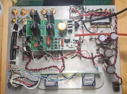
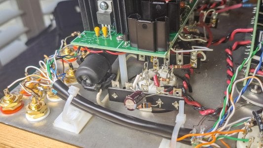
After completing the upgrade PCB installation I performed all the voltage tests from the manual and everything passed. I then finished the Claymore board installation and powered it on. On the first power on, I had sound on one channel only. I moved the RCA cables around and briefly got sound on both channels for about 3-4 minutes, then both channels went completely silent and haven't come back since. The tubes are still glowing normally.
This is what I could verify.
Could this be a failed Q2A (MJE5731A)? Or is there something else I should be looking at?
Thank you!
Alan B
I recently completed the Moreplay Upgrade Kit. I´m hoping you can help me figure out what's going on.
After completing the upgrade PCB installation I performed all the voltage tests from the manual and everything passed. I then finished the Claymore board installation and powered it on. On the first power on, I had sound on one channel only. I moved the RCA cables around and briefly got sound on both channels for about 3-4 minutes, then both channels went completely silent and haven't come back since. The tubes are still glowing normally.
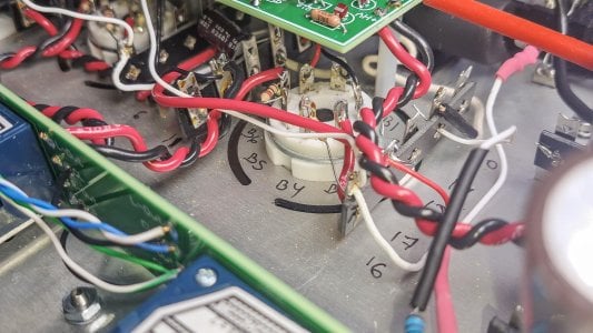
This is what I could verify.
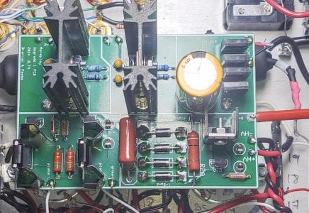
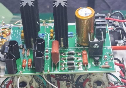
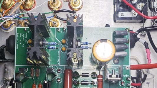
- All signal path wiring continuity checks: passed
- Component orientations (Q2A/B/C, ZD1-ZD4): visually verified correct
- LM1085 and MJE5731A position are correct
- White wire continuity from 16U to Plate B and 6U to Plate C: confirmed
- D1A and D2A: lit
- D1B and D2B: not lit
- A2 to A7: 6.28V
- B2 to B7: 6.25V
- Terminal 21: 303V
- Terminal 23: 0V
- +HV on PCB: 303V
- -HV on PCB: 0V
- B+ Reg TP: 3V (expected 175-180V)
- Terminal 6U: -0.5V (expected 120-140V)
- Terminal 16U: -0.5V (expected 120-140V)
- Plate B on PCB: spikes to 30V for ~2 seconds then collapses to 1.66V
- Plate C on PCB: spikes to 30V for ~2 seconds then collapses to 1.35V
- 2.2uf capacitor in the PCB: spikes to 30V for ~2 seconds then collapses to 3V
- Note: when preamp is powered off, voltages slowly rise back up to 14-20V then gradually discharge
Could this be a failed Q2A (MJE5731A)? Or is there something else I should be looking at?
Thank you!
Alan B
Last edited: